Semiconductors like silicon and germanium have been getting a bit long in the tooth lately.
The electrons within these materials do not move as fast as microchip engineers would like them to.
They've tried to work around this by adopting progressively smaller manufacturing processes, that allow for more transistors in the same place.
However we are already approaching atomic scales and when things get so small strange
quantum effects begin to occur that lead to the chip not working as intended and putting out too many errors.
A commercial quantum computer does not yet appear to be presented anytime soon, so the microchip manufacturers have been researching for some time with photonics, the science of light. Here I will present three of the most important of these advances of three companies, Intel, Luxtera and IBM.

Image from Intel
Intel's Light Peak project was not designed to crunch numbers in CPUs, only to move data around. It is targeted as a universal optical interconnect, intended to replace all electrical connectors, even the fastest ones like USB3 and HDMI. Intel has other projects researching real silicon photonics (light beams in bed with silicon) in CPUs but they are not yet ready for commercial use. Light Peak though is almost there, and we could see the first products already in 2011. Although this image looks quite impressive, Light Peak's specs do not.
It is scheduled to be initially rolled at a mere 10 Gbit/s speed, just double that of USB3 and just shy over what HDMI 1.3+ can achieve. Obviously the bottleneck lies in its electric components; or Intel does not want it to compete with its professional Infiniband interconnect which can reach a blazing 300Gbit/s speed in its upcoming EDR/12x flavour.
Light Peak is ultimately aimed for a top speed of 100 Gbit/s "over the next decade".

Image source
Luxtera is currently in the optical cable business but also agressively researches chip level silicon photonics, much like Intel and IBM. This is the Blazar Lux5010A, a quadruple optical cable boasting 40(4x10) Gbit/s speeds. Already on sale and surpassing Light Peak (though it is obviously pro oriented and quite more expensive than what LP will cost), not bad at all.

Image source
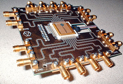
This one is an older prototype test board for Luxtera's silicon photonics future chips and optical chipset interconnects. It appears to be similar to Light Peak and it is also specced at 10 Gbits/s.
But still, no word on replacing the intricate copper wires inside CPUs with microfiber optics.
They are suppossed to be researching this but they have not yet announced anything solid.
So, last but certainly not least, the really exciting stuff, the latest announcement on the field from IBM:
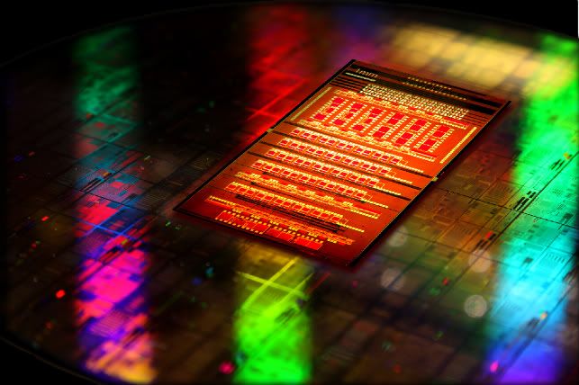
Image from IBM
This doubtlessly impressive image is what the photonics team of IBM announced on December the 1st. It is a pure silicon photonics chip (placed on a conventional silicon wafer), with optical and electrical elements coupled tighter and in a smaller space than what had ever been achieved before.
This is a prototype chip, intended to be a building block for future exascale-class supercomputers. According to IBM's Solomon Assefa, a member of the research team at IBM's Watson Research Center in Yorktown Heights, New York, "We need faster ways to shuttle information around. Our main motivation is to build, in five years or so, exascale systems that will be 1,000 times faster than what we have now."
Conclusion
The US Department of Energy and scientists like biologists, astrophysicists and chemical engineers, all crave for faster supercomputing speed. For the rest of us let me remind you that the supercomputers of today are the computers of tomorrow. So eventually we will have this technology in our own personal devices too. Next year we will most likely be treated to the fist Light Peak products and presumably by the end of the decade we will also have beautiful glowing chips like this one in our smartphones or tablets. I can't wait!
© 2010, Nikolaos D. Skordilis
Sources:
Excellent Design and layout blog. i like this blog and this is very informative. Chip level training in hyderabad
ReplyDelete